Service Mode
Three Cooperation Models
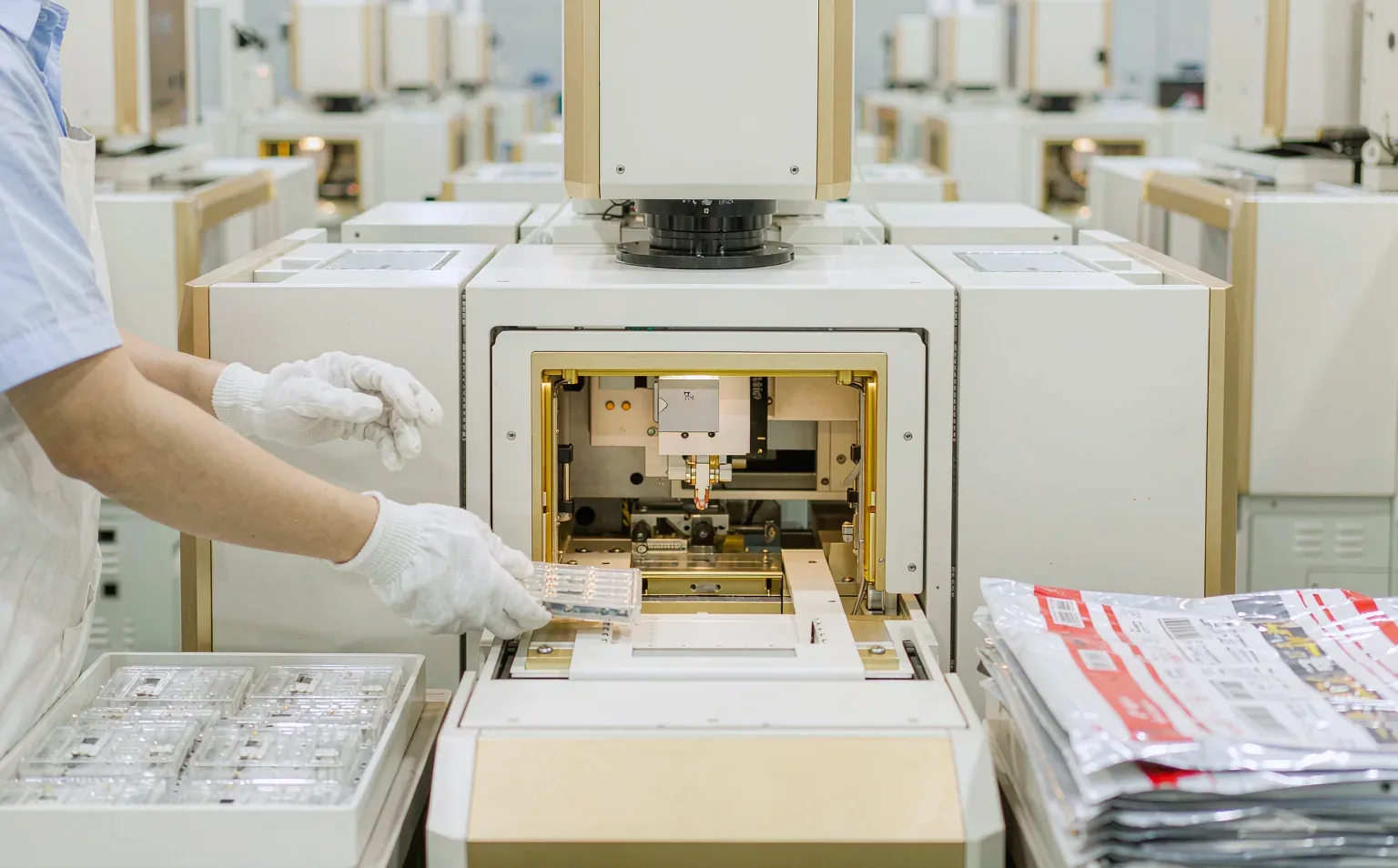
Consigned Assembly
You supply the key parts — we run the whole process with transparent per-step pricing.
- Flexible supply: you provide ICs, connectors and other key parts; stencils, solder paste and passives can be sourced on your behalf
- Full process: SMT placement, DIP insertion, wave soldering and firmware flashing
- Incoming control: MQC counting and baking/dehumidifying; shortages flagged 3 working days in advance
- Flexible scheduling: phased material delivery and batch production to ease inventory pressure
- Ideal if you have stable material channels or franchise pricing
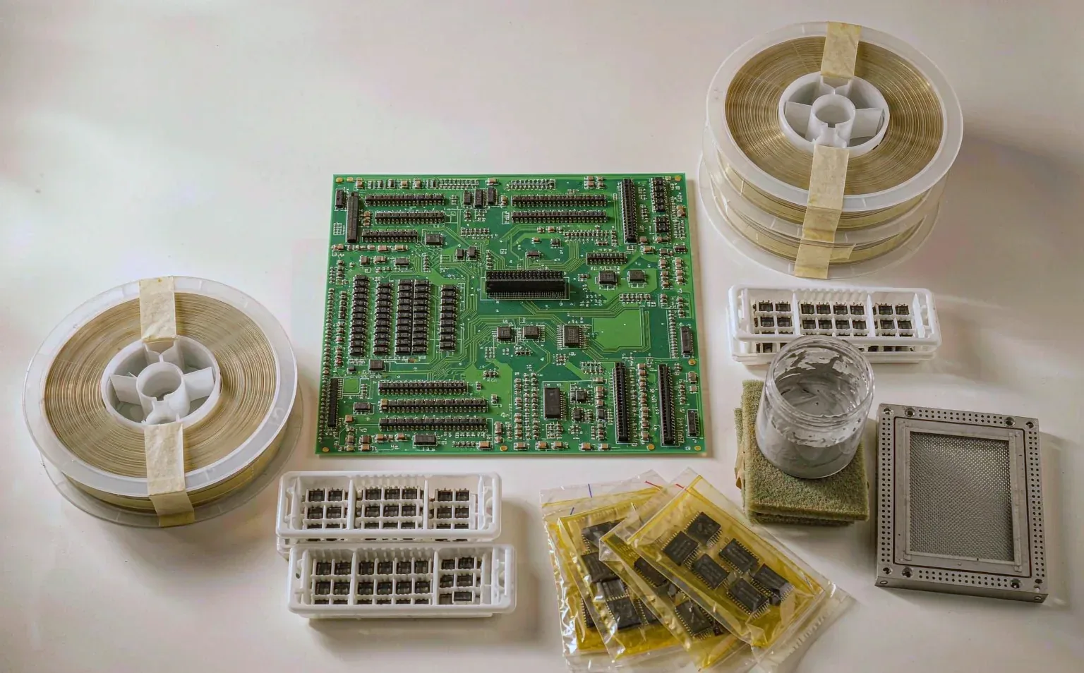
Turnkey
BOM sourcing + PCBA assembly in a single order — simple and worry-free.
- One-stop sourcing: all parts procured from manufacturers / franchise channels, with alternates suggested for shortages
- Better cost: no multi-vendor purchasing, transfers or re-counting
- Controlled lead time: shortages resolved via alternates or allocation to protect your schedule
- Simple settlement: material cost and labor on one quotation sheet
- From BOM to finished boards in one delivery — ideal if you want zero middle-step hassle
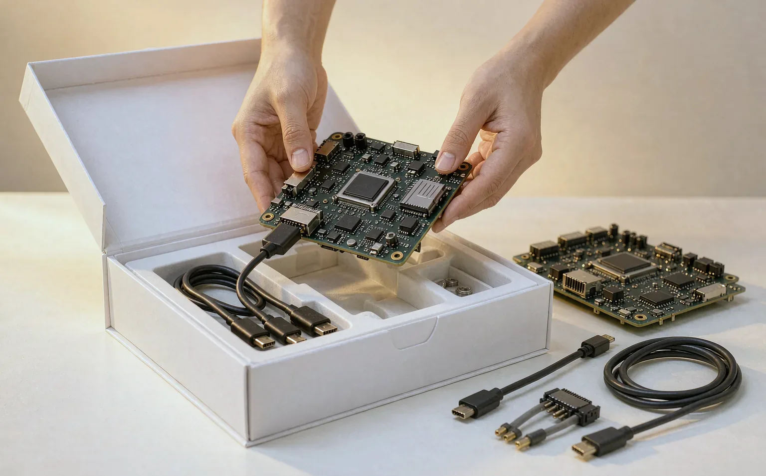
Full-Process Delivery
From design to finished goods — you receive sellable products.
- Development: schematic design, PCB layout and firmware, all in one place
- Manufacturing: sourcing + placement + flashing + box-build assembly
- Quality assurance: conformal coating, burn-in and FCT functional testing, fully inspected
- Ship-ready: retail packaging and white-label shipping, direct to your customers
- Ideal if you focus on market and sales without an in-house production team